Quantum Computer Integrated into Microscope to Advance Electron Imaging
A new wave of research is fusing quantum computing directly with electron microscopy — a convergence that promises to shatter long-standing limits on what scientists can see and measure at the atomic scale. The implications range from drug discovery to next-generation semiconductors to the design of materials that barely exist yet.
The Science: Qubits Meet Electron Beams
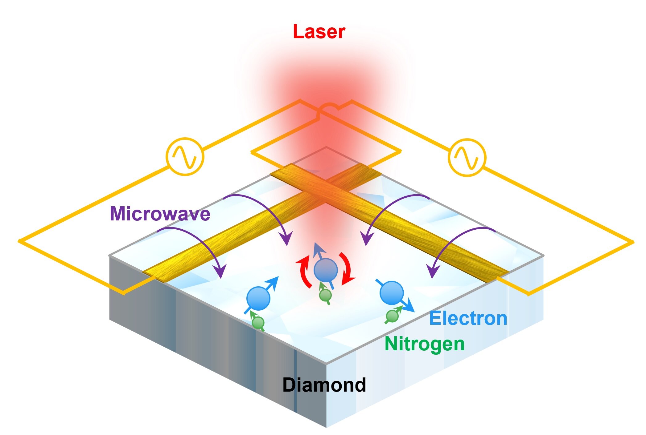
The core idea is elegant but technically demanding: map the physics of electron microscopy onto quantum circuits, then let a quantum computer do the image-formation mathematics that classical hardware struggles to perform efficiently.
Researchers Sean D. Lam of Colorado College and Roberto dos Reis of Northwestern University's NUANCE Center have published a framework that does exactly this. Their work, detailed in a preprint at arxiv.org, recasts phase-contrast transmission electron microscopy (CTEM) — one of the most powerful tools in materials science — as a gate-based quantum circuit. The electron wavefield is amplitude-encoded onto a register of qubits, while key imaging steps like free-space propagation and lens aberration correction are implemented using quantum Fourier transforms and phase operators. The result is a physics-grounded pipeline that a fault-tolerant quantum processor can run end-to-end.
Separately, a team around Hiroshi Okamoto has demonstrated that this quantum computational approach yields a provable advantage specifically in low-dose electron microscopy — experiments where the electron beam must be kept weak to avoid destroying fragile biological or organic specimens. As explained in their analysis covered by Quantum Zeitgeist, fewer quantum "queries" to the sample means less radiation damage, which means more usable data extracted before a specimen degrades. That is not an incremental improvement — it is a structural one baked into the mathematics of quantum query complexity.
An earlier theoretical foundation, Universal Quantum Electron Microscopy, laid out the case for provable quantum advantage in this context. The 2026 experimental and algorithmic work is now moving that concept toward practical implementation.
The Hardware: Instruments Getting Smarter
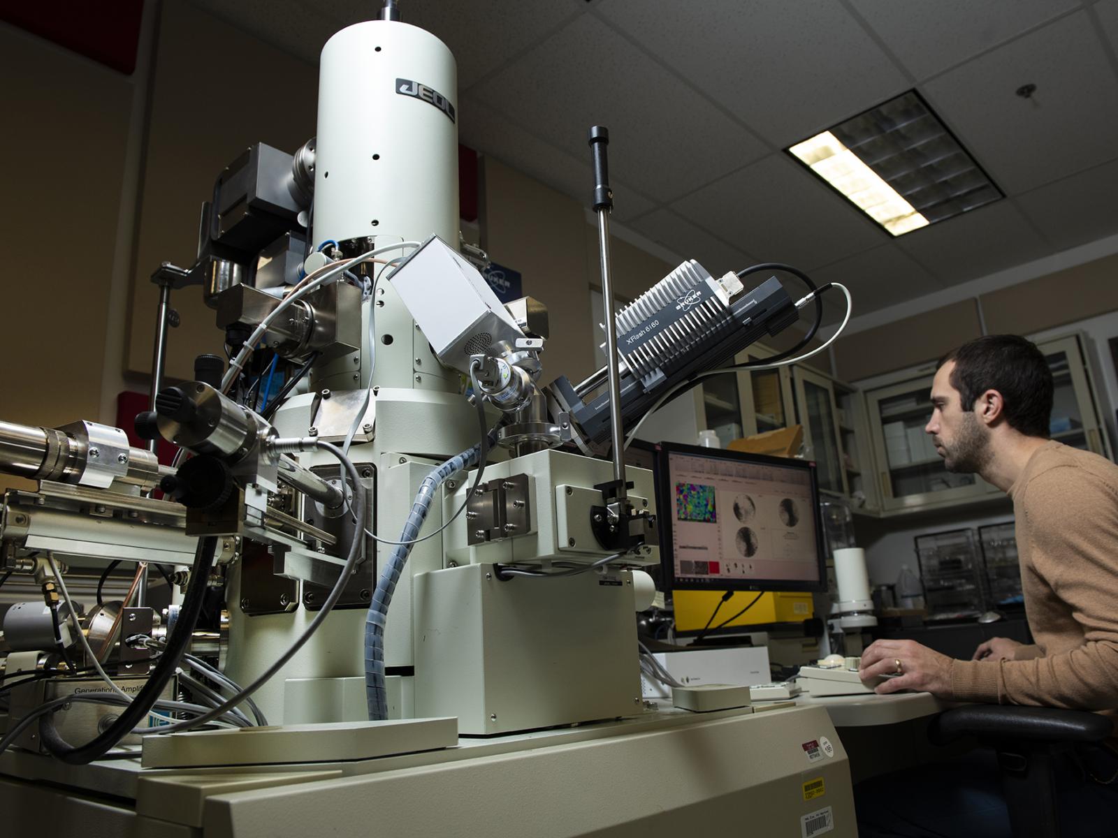
On the instrument side, the United States is not waiting for full-scale quantum integration to push electron microscopy forward. Brookhaven National Laboratory has installed a new scanning transmission electron microscope at its Center for Functional Nanomaterials — one that delivers 200 times better energy resolution than conventional instruments. Operating at voltages as low as 20 kiloelectron-volts (far below the typical 100–300 keV range), it minimises beam damage while simultaneously mapping a material's atomic structure, chemical composition, and electronic behaviour. It can resolve quasiparticles — phonons, magnons, plasmons — that were previously blurred into noise.
Meanwhile, the Technion in Israel has opened a dedicated Quantum Microscopy Lab, an interfaculty effort pairing quantum optics expertise with electron-beam instrumentation. Argonne National Laboratory's Center for Nanoscale Materials is operating the Quantum Emitter Electron Nanomaterial Microscope (QuEEN-M), which integrates cathodoluminescence and photoluminescence spectroscopies directly with a probe-corrected scanning transmission electron microscope — a systems-level fusion rather than a bolt-on upgrade.
Why It Matters
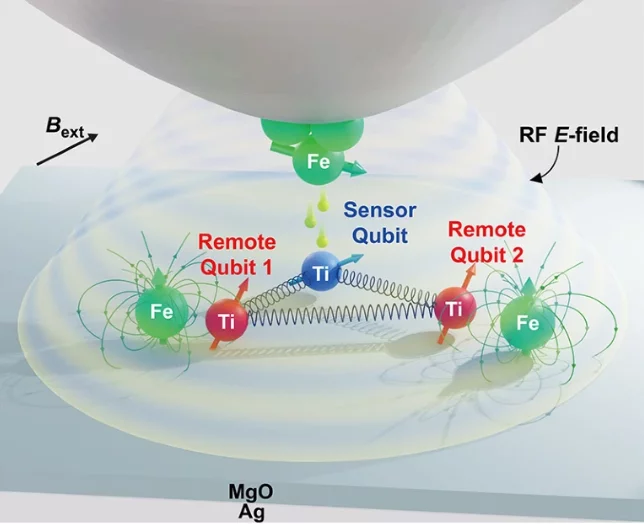
The stakes are highest wherever atomic-scale imaging intersects with precision — which is nearly everywhere in frontier science. Beam-sensitive specimens like proteins, organic semiconductors, and battery electrode materials have historically been the hardest to image well: too much electron dose and the sample is destroyed before a clear picture forms. Quantum-enhanced algorithms could change that calculus fundamentally, enabling researchers to extract structural data from samples that were previously considered too fragile to study at this resolution.
For the semiconductor industry, the implications are just as significant. As chip geometries shrink below two nanometres, characterisation tools need to keep pace. An electron microscope that can simultaneously assess atomic structure, electronic behaviour, and quasiparticle dynamics — informed by quantum computation — is not a laboratory curiosity. It is the kind of instrument that determines whether a next-generation transistor design works or fails.
The convergence is still early. Fault-tolerant quantum computers capable of running these circuits at scale remain years away from routine laboratory use. But the theoretical groundwork is solid, the algorithmic advantage is provable, and the hardware investments are already underway.
Key Takeaways
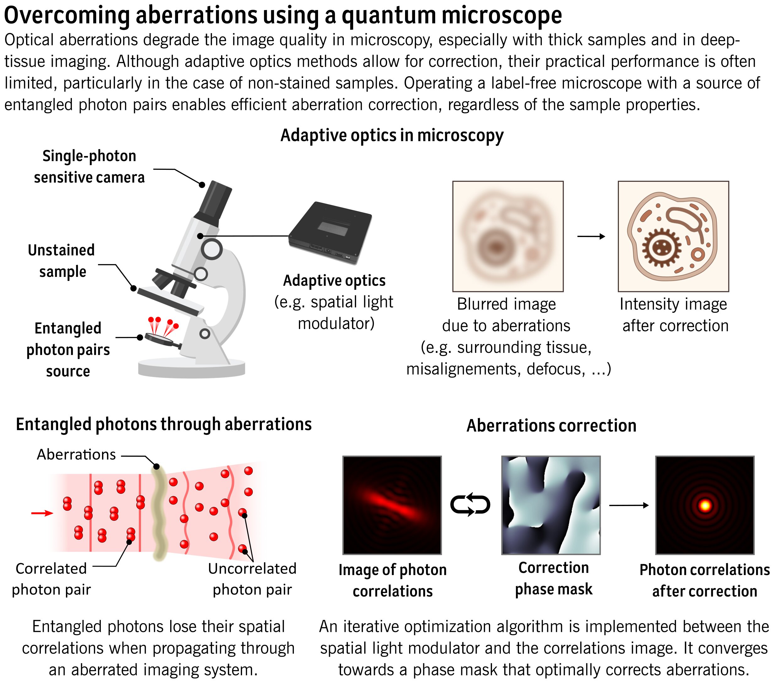
- Quantum circuits can now model electron microscopy end-to-end, with researchers at Colorado College and Northwestern University demonstrating a gate-based framework that maps CTEM physics directly onto qubit registers.
- Low-dose imaging stands to benefit most: quantum query complexity offers a provable advantage when the electron beam must be kept weak to protect delicate specimens, extracting more information with less damage.
- Physical instruments are advancing in parallel — Brookhaven's new microscope achieves 200× sharper energy resolution, and Argonne's QuEEN-M platform integrates quantum-optical spectroscopy with electron microscopy at the systems level.
- The path to routine quantum-enhanced microscopy is real but not immediate, requiring fault-tolerant quantum hardware to fully realise algorithmic gains — though the theoretical and experimental foundations are now firmly in place.
Sources:
- Low-dose Image Recognition with Quantum Computational Electron Microscopy (arXiv)
- Quantum Circuits Simulate Electron Microscope Images Accurately (Quantum Zeitgeist)
- Universal Quantum Electron Microscopy: A Small-Scale Quantum Computing Application with Provable Advantage (arXiv)
- US installs electron microscope with 200x sharper energy resolution (Interesting Engineering)
- Toward a New Era in Electron Microscopy and Medical Imaging (Technion UK)
- Groundbreaking Electron Microscope Installed at CFN (Brookhaven National Laboratory)